The tiny copper wires that connect different areas of an integrated
circuit may soon limit microchip-processing speeds. So European
researchers have developed technologies to produce and combine
semiconductor microlasers with silicon wave guides for novel,
power-efficient optical connections.
We have all experienced the effect of Moore's Law: almost from the
second you unpack a newly purchased computer it is already outdated.
The next model – with faster processing power and more advanced
features – is already in the shop.
Gordon E. Moore, co-founder of Intel, described the phenomenon of
microchip miniaturisation in 1965 when he observed that the number of
transistors you can fit into an integrated circuit appeared to double
about every two years.
The microelectronics industry still follows this “law”, but unless
new fabrication or microprocessing technologies are quickly developed
this relentless miniaturisation may peter out in less than a decade.
Microchips based on silicon wafers are nearing their theoretical limits
as physical properties of near nanoscale silicon integrated circuits begin to interfere with their performance.
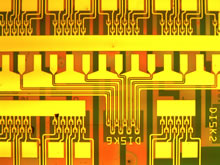
The speed of data transfer within integrated circuits is one of the
major bottlenecks. At present, to pass information from one part of a
chip to another, the data packet is sent as electrons through copper
wires, known as copper interconnects.
These wires may be just a few millimetres in length, but for the
electrons it is like running between underground trains at rush hour.
The electrons must all squeeze down narrow tunnels while a crowd backs
up at the entrance.
Copper can’t cope
“Copper-wire
interconnects place serious limitations on the performance of silicon
integrated circuits,” says Dries Van Thourhout from Ghent University's
Photonics Research Group and Belgium's micro- and nanoelectronics
research centre IMEC. “It is hard to transmit data down these
interconnects in a sufficiently fast, power-efficient way. It is a
problem of bandwidth and copper will not be able to cope with the
processing power of tomorrow's microchips.”
Optical interconnects use light instead of electrons to represent
information; they are a highly appealing alternative to copper
interconnects, with the potential to be far more efficient,
transmitting more data but using the same or even less power.
Instead of travelling along copper wires, photons travel the
distance between source and detector along wave guides, like miniature
optical fibres. At this scale, however, the wave guides are made out of
silicon rather than glass.
“Lots of research has shown that you can etch wave guides for
photons into silicon,” says Van Thourhout. “This is great because you
are using the same materials and fabrication technologies as you do to
make integrated circuits. But there is one significant drawback: it is
extremely hard to get light out of silicon.”
Despite extensive research to exploit many of silicon's peculiar
properties, it is highly unlikely that purely silicon-based lasers will
reach efficiency comparable to that of their semiconductor-based
cousins for the foreseeable future.
Van Thourhout has coordinated a European consortium that has
successfully combined the best of both worlds: silicon wave guides and
microscale lasers made from a semiconductor call indium-phosphate. The PICMOS project
was a partnership between several European research institutions,
universities and two French companies STMicroelectronics and TRACIT
Technologies, now owned by Soitec.
Mini-laser system
Part of the research
involved the fabrication of a miniaturised laser system small enough to
generate light for each interconnect. The EU-funded PICMOS team
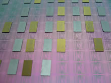
developed a method to etch indium-phosphate lasers with a diameter of
just 7μm, sufficiently small to integrate several thousand onto a 2cm x
2cm silicon chip. This is the first time that such compact lasers have
been produced in a very practical, cost-efficient way.
The tiny lasers could also have applications in miniature optical
sensors, such as strain detectors, or be used to build incredibly
cheap, but very powerful optical biosensors. But the biggest
breakthrough in the project was the development of a bonding technology
that joins the silicon and iridium-phosphate materials together.
“The bonding process, now transferred to TRACIT, effectively 'glues'
the silicon and semiconducting indium-phosphate in layers. It is
possible to etch out the microlasers and the silicon wave guides and
produce an optical interconnecting layer,” says Van Thourhout. “The
bonding process and the refinement of the microlaser and the
accompanying detectors have been major breakthroughs.”
The production cost of the prototype optical interconnect layer is
still too high for mass production, although the results from the
demonstrator 'chip' have been extremely encouraging. A follow-up
project, WADIMOS, will continue to drive the PICMOS platform towards
commercialisation. In particular it will develop a pilot line that
integrates the fabrication of the optical interconnect layer into the
regular integrated circuit manufacturing process.
“We envisage a layer on an integrated circuit that sits on top of
the classical etched copper electrical interconnect layer,” says Van
Thourhout. “This optical interconnect layer would be less sensitive to
temperature, immune from electromagnetic noise, and have lower power
consumption. Meanwhile, the bonding system could be adapted for many
other electronics applications, for example to stack integrated
circuits and in microfluidic technologies. The application of the
PICMOS platform could be tremendous for tomorrow's chip technologies
and wide-ranging in many other associated applications.”