|
| |
It's a small world...
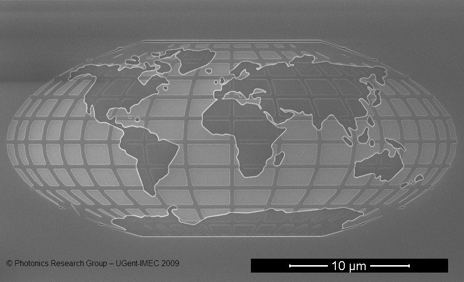
The small world as seen through a scanning
electron microscope.
The Photonics Research Group of Ghent University-IMEC has
fabricated a world map on a scale of 1 trillionth. Using CMOS fabrication tools, IMEC has reduced the
40-thousand-kilometer circumference at the equator down to 40 micrometer, about
half the width of a human hair. The map is put in a corner of a optical silicon
chip designed for one of the group's research projects on nanophotonic
integrated circuits. The scale reduction enables more complex optical functions on a single
chip for applications in telecommunication, high-speed computing, biotechnology
and health-care. Noteworthy, the factor of 1 trillion corresponds to the scale
prefix Tera (like in Terabyte), but in this situation it would be better to call
it ‘Terra’-scale.
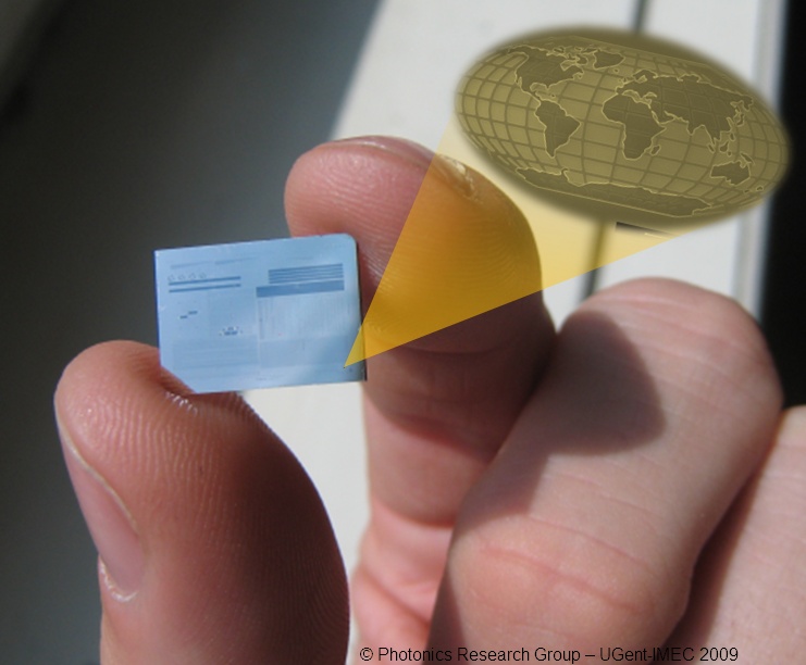
Scale of the world map. It is hidden in the
bottom right corner of a photonic chip.
On the technical side
-
The world map was defined on a silicon photonics
test chip in IMEC’s clean-room for 200mm processing, using the same
high-resolution optical lithography techniques as used for microelectronics
fabrication, and the fabrication consisted of a 30-step process including layer
depositions and chemical etching steps on a silicon-on-insulator wafer. Four
different layer thicknesses can be resolved, corresponding to four different
images, or mask layers, that have to be patterned separately. The tiny world map
was piggy-backed onto a test and development chip for new nanophotonic
circuitry.
-
The silicon photonics technology that is being
developed with these chips integrates optical circuits onto a small chip: Light
can be manipulated on submicrometer scale in tiny strips of silicon called
waveguides or
photonic wires. Using the unique
properties of silicon, combined with state-of-the-art manufacturing technology,
these silicon photonic circuits can pack a million times more components on the
same footprint as today’s commercial glass-based photonics.
-
The circuits developed on this particular chip
were used to demonstrate photonic wires with the lowest propagation losses.
Also, structures were developed to improve the efficiency of coupling light from
the outside world (like an optical fiber) to the wires on chip.
-
To put it in perspective, the smallest features resolved on the
map are about 100 nanometer (corresponding to 100km), which is
still a several times larger than the today’s state-of-the-art
transistors.
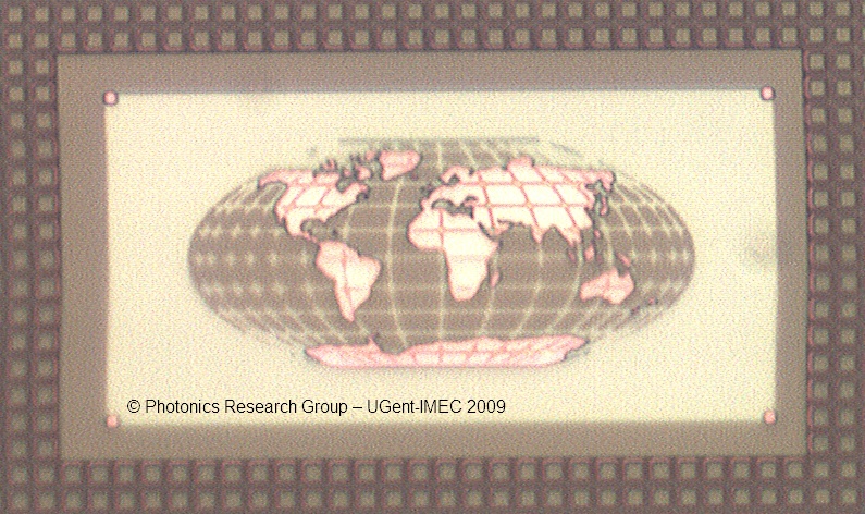
The small world as seen through an optical
microscope. The different colors are caused by interference effects in the
different layer thicknesses of Silicon.
The Photonics Research Group is a 60-people strong
laboratory of Ghent University (Ghent, Belgium) and is associated with the Interuniversity
Microelectronics Center (IMEC), located in Leuven, Belgium. The group focuses on the
research and development of smart photonic chips for future application in
communications, identification, biosciences and health care, building on
technologies developed for the microelectronics industry. The use of silicon and
microelectronics fabrication can drastically reduce the size, power consumption
and cost of photonic chips, bringing them closer to integration with consumer
electronics, cell-phones as well as smart distributed sensor networks and
point-of-care diagnostics.
Links
Photonics group:
photonics.intec.ugent.be
Ghent University: www.ugent.be
IMEC: www.imec.be
Contact:
Wim Bogaerts.
wim.bogaerts@intec.ugent.be,
+32-9-264 3324
Acknowledgements
World map design: Wim Bogaerts
Design support: Pieter Dumon, Jin Guo
Fabrication Process: Shankar Kumar Selvaraja, Peter Verheyen
Images: Dirk Taillaert, Liesbet Van Landschoot
and all the people at Ghent University and IMEC who contribute to the results of
Photonics Research Group.
Relevant publications
P. Dumon, W. Bogaerts, A. Tchelnokov, J.-M. Fedeli, R. Baets,
Silicon Nanophotonics,Future
Fab International (invited), 25, p.29-36 (2008)
P. Dumon, W. Bogaerts, R. Baets, J.-M. Fedeli, L. Fulbert,
Towards foundry
approach for silicon photonics: silicon photonics platform ePIXfab,Electronics
Letters (invited), 45(12), p.581-582 (2009)
S. Selvaraja, P. Jaenen, W. Bogaerts, P. Dumon, D. Van Thourhout, R. Baets,
Fabrication of Photonic
Wire and Crystal Circuits in Silicon-on-Insulator Using 193nm Optical
Lithography,Journal of Lightwave Technology, 27(18), p.4076-4083 (2009)
Coverage
We got picked up by
Wired.com and now
Gizmodo as well, and that feed got mirrored by
many others.


|