|
| |
Nanophotonic devices in bonded InP-membraneMain Researcher: Frederik Van Laere
InP/InGaAsP material is the workhorse for opto-electronic devices for telecom applications. However, a typical InP-based heterostructure has also some disadvantages, especially for passive components. They often require deep etching, which is difficult in a lot of cases. Additionally, due to the medium refractive index contrast, bending radii and other passive components (e.g. grating couplers) can't be made very small, compromising large scale integration of components.
The vertical index contrast can be modified by applying wafer bonding. In our case, the resulting structure consists of a thin InP-membrane on a low-index polymer BCB (n=1.54). This layer structure is optically very similar to Silicon-on-Insulator(SOI). Deep etching is not longer required, and components can be made as compact as is the case for SOI-devices.
The high vertical index contrast can then be used for components requiring this high contrast, which can still be integrated with (membrane type) classical InP-based layer structures for active devices.
We have transferred the principle of grating couplers to this InP-membrane platform. A gold mirror below the grating substantially improves the coupling efficiency. These gratings will be further integrated with other passive components (e.g. wavelength selective components) and photodetectors.
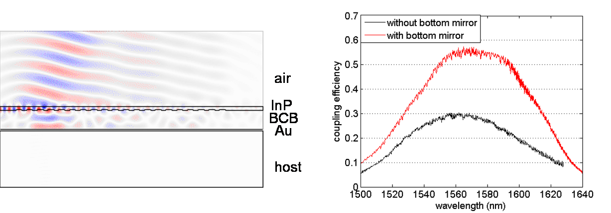
(Left) Simulation of an InP-membrane grating coupler with gold bottom mirror. (Right) Measurement result
Other people involved: Related Research Projects
PublicationsInternational Journals
-
T. Spuesens, F. Mandorlo, P. Rojo-Romeo, P. Regreny, N. Olivier, J.M. Fedeli, D. Van Thourhout,
Compact integration of optical sources and detectors on SOI for optical interconnects fabricated in a 200 mm CMOS pilot line, Journal of Lightwave Technology, 30(11), p.1764-1770 doi:10.1109/jlt.2012.2189871 (2012)
 . . -
F. Van Laere, T. Stomeo, C. Cambournac, M. Ayre, R. Brenot, H. Benisty, G. Roelkens, T. F. Krauss, D. Van Thourhout, R. Baets,
Nanophotonic polarization diversity demultiplexer chip, Journal of Lightwave Technology, 27(4), p.417-425 doi:10.1109/jlt.2008.929414 (2009) .
-
F. Van Laere, T. Stomeo, D. Taillaert, G. Roelkens, D. Van Thourhout, T.F. Krauss, R. Baets,
Efficient Polarization Diversity Grating Couplers in Bonded InP-membrane, IEEE Photonics Technology Letters, 20(4), p.318-320 doi:10.1109/lpt.2007.915587 (2008) .
-
G. Vecchi, F. Raineri, I. Sagnes, K.H.-Lee, S. Guilet, L. Le Gratiet, F. Van Laere, G. Roelkens, D. Van Thourhout, R. Baets, A. Levenson, R. Raj,
Photonic-crystal surface-emitting laser near 1.55 µm on gold-coated silicon wafer, Electronics Letters, 43(6), p.343-345 doi:10.1049/el:20073816 (2007) .
-
G. Vecchi, F. Raineri, I. Sagnes, K-H. Lee, S. Guilet, L. Le Gratiet, A. Talneau, A. Levenson, R. Raj, F. Van Laere, G. Roelkens, D. Van Thourhout, R. Baets,
High contrast reflection modulation near 1.55 um in InP 2D photonic crystals on silicon wafer, Optics Express, 15(3), p.1254-1260 doi:10.1364/oe.15.001254 (2007) .
-
F. Van Laere, M. Ayre, D. Taillaert, D. Van Thourhout, T. F. Krauss, R. Baets,
Compact and efficient fibre-to-waveguide grating couplers in InP-membrane, Electronics Letters, 42(6), p.343-345 doi:10.1049/el:20064128 (2006) .
International Conferences
-
M. Tassaert, S. Keyvaninia, D. Van Thourhout, W.M.J. Green, Y. Vlasov, G. Roelkens,
A nanophotonic InP/InGaAlAs optical amplifier integrated on a Silicon-On-Insulator waveguide circuit , Information Photonics 2011, Canada, doi:10.1109/ico-ip.2011.5953699 (2011) .
-
F. Van Laere, T. Stomeo, D. Taillaert, D. Van Thourhout, T. F. Krauss, R. Baets,
Polarization diversity grating couplers in bonded InP-membranes, PECS VII, United States, (2007) .
-
H. Benisty, L. Martinelli, O. Khayam, M. Ayre, M. Kotlyar, T. F. Krauss, M. Midrio, R. Brenot, G. H. Duan, F. Van Laere, D. Van Thourhout, K. Janiak, H. Heidrich, M. Kamp, R. Houdre, L. A. Dunbar, D. Gallagher,
Photonic-crystal-based optical functions for metropolitan area networks: polarisation control, linear amplification, wavelength selection, 32nd European Conference on Optical Communication (ECOC), 2006, p. We 1.2.2, doi:10.1109/ecoc.2006.4801133 (2006) .
-
F. Van Laere, M. Ayre, D. Taillaert, D. Van Thourhout, T. F. Krauss, R. Baets,
Compact and highly efficient grating couplers between optical fiber and nanophotonic waveguides in bonded InP-membranes, 32nd European Conference on Optical Communication (ECOC), 2006, p Tu 1.4.5, doi:10.1109/ecoc.2006.4801040 (2006) .
-
F. Van Laere, M. Ayre, D. Taillaert, D. Van Thourhout, T. F. Krauss, R. Baets,
Compact and efficient fiber-to-waveguide grating couplers in InP-membrane, SPIE Photonics Europe, 6182, France, p.174 doi:10.1117/12.668232 (2006) .
-
F. Van Laere,
Compact grating couplers in InP, ePIXnet Winter School, Optoelectronic Integration - Technology and Applications, Switzerland, p.45 (2006) .
National Conferences
-
F. Van Laere, T. Stomeo, D. Van Thourhout, T. F. Krauss, R. Baets,
Efficient Polarization Independent Optical Link in Bonded InP-membrane, 8th FirW PhD Symposium, Interactive poster session, paper nr. 38 (proceedings available on CD-ROM), Belgium, (2007) .
Back to overview
|