|
|
|||||
| intern | ||||||
|
|
||||||
| ||||||||||
back to vacancy list Vacancy: Visible and near-IR lasers on a chip (Open)Posted on 9/5/2025ContextThe visible and near-infrared (near-IR) wavelength range (400 nm - 1100 nm) is the region of interest for a large number of biomedical applications, environmental sensing applications and emerging applications such as in the field of quantum sciences. Applications include optical coherence tomography, flow cytometry, environmental sensors to detect water pollution, quantum computers and atomic clocks. These applications will benefit from an integrated active photonic platform at visible and near-IR wavelengths. One of the challenges is that these applications need widely spaced wavelengths, sometimes spanning as much as an octave, in the same system. At the same time these systems tend to be complex. Here, we will leverage the existing silicon nitride platform technology by integrating active building blocks on the platform to enable these non-telecom applications. 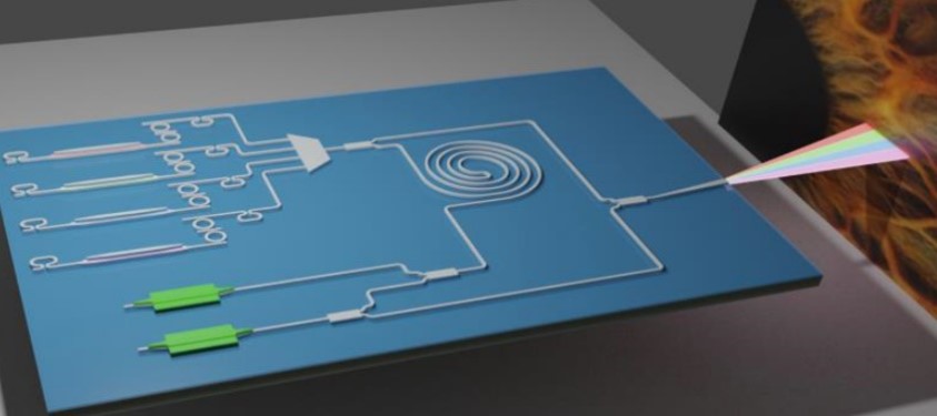 Job DescriptionBuilding further on the first results obtained at Ghent University, a new generation of broadband and narrow linewidth lasers emitting in the visible and near-IR ranges will be developed in this postdoc-project. This include: the design of the SiN/III-V heterogeneous systems, the integration of the GaAs and GaN III-V amplifiers on SiN circuits using transfer printing technology, the testing of the fabricated devices. Candidate Profile- You have a MSc degree in Science or MSc in Engineering
About UsThe Photonics Research Group (about 85 people) is associated with IMEC, and is part of the Department of Information Technology of Ghent University. The group is headed by Prof. R. Baets and has been active in photonics device research for many years. The other professors in the group are P. Bienstman, W. Bogaerts, B. Kuyken, N. Le Thomas, G. Morthier, G. Roelkens and D. Van Thourhout. The main research directions are silicon nanophotonics, heterogeneous integration, optical communication, photonic (bio)sensors and photonic integrated circuits for biomedical applications in the near-infrared and mid-infrared wavelength range. More in particular, the silicon nanophotonics work focuses on the design and fabrication of SOI-based photonic devices using standard lithographic techniques compatible with CMOS-processing.
How to apply?Mail CV and Motivation letter to:
More information
|