|
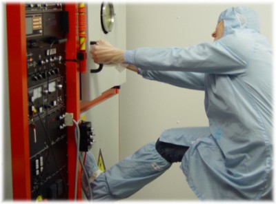
Since June 2004 the processing facilities of the Photonics Research Group are located
in the new cleanroom built by Ghent University at the "Technology Centre
Zwijnaerde", just outside of the center (see also: How to reach us). The cleanroom has a
surface of approximately 1100 square meters, of which the Photonics Research Group can use
approximately one third. The focus is on compound semiconductor based devices, both on InP
and GaAs substrates. In addition, we work on the fabrication and assembly of micro-optical
structures for optical interconnect applications.Below you’ll find a short overview
of our most relevant equipment. For more details, information or processing requests
contact driesvt@intec.ugent.be or steven.verstuyft@intec.ugent.be .
Standard equipment includes:
- High resolution photolithography down to 0.6 um linewidth (Karl Suss MA6 & MJB3
maskaligners).
- Plasma enhanced chemical vapour deposition of dielectric films (e.g. silicon dioxide,
silicon nitride)
- Evaporation and sputtering of metal contacts
- Plasma etching and Reactive Ion Etching
- Deposition of dielectric coatings (AR and HR)
- Flip-chip device mounting
- Wafer thinning and polishing
Advanced tools include:
|
|
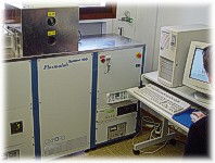
- An inductively coupled plasma etch system for the fabrication of high-quality deeply
etched waveguide structures.
|
 |
- Holographic fabrication of grating structures
- Both one and two dimensional grating structures
- Using Argon laser
- Grating period varying from 250 nm to 2 µm
|
|
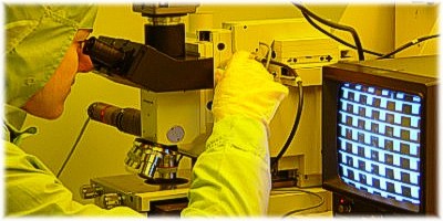
- Measurement Microscope
- Die-to-wafer bonding proces
- Suitable for double sided processing (e.g. ring
resonators) and for the heterogeneous integration of III-V semiconductor material and
silicon circuits ( e.g. SOI research)
- Using Benzocyclobuthene (BCB) as intermediate layer
|
|
- Oxidation of AlGaAs films
- For the fabrication of high-vertical contrast optical waveguides
- For the fabrication of integrated beam-expanders (PhD Kurt de Mesel)
|
 |
- SEM (JEOL) Jointly operated with the ELIS-department
|
|
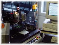
- Laser ablation system
- For the structuring of a wide variety of materials
- With excimer laser operating at either 193 nm or 248 nm
|
 |
All MOCVD activities were moved to IMEC Leuven during 2002. III-V substrates for the
fabrication of optoelectronic devices are now obtained from other research groups or from
commercial wafer fabs.
The photonics research group together with 6 other UGent research groups received a
grant from the Flemish government for buying a dual beam FIB (focused ion beam). The FIB
arrived in early spring 2005.
|