|
|
|||||
| intern | ||||||
|
|
||||||
| ||||||||||
Optical fiber probe for photonic integrated circuitsMain Researcher: Stijn Scheerlinck An important step towards widescale applications of photonic integrated circuits is the ability to test the operation and performance of circuit parts and components on a wafer-scale. In microelectronics manufacturing, probes exist in the form of metal tips and are widely used for wafer-scale, non-destructive and parametric testing. An optical equivalent does not yet exist.

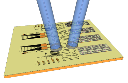
Artist We propose a metal grating based optical fiber probe for photonic integrated circuits. The device is based on a single-mode fiber containing a sub-wavelength period metal grating on the facet. When approaching an integrated waveguide, light can be efficiently coupled between probe and waveguide without the need for integrated coupling structures, paving the way for wafer-scale circuit testing. 
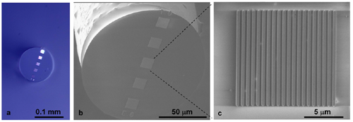
(a) Microscope image of the fiber probe facet containing 10 x 10 m gold gratings. (b) SEM picture of the fiber facet. The middle grating is aligned to the core. (c) Detail of the gold grating. A nanoimprint and transfer process was developed for fabricating this probe in a single step. We reported 15 % coupling efficiency between a gold grating fiber probe and a 220 nm x 3 um silicon-on-insulator waveguide and demonstrated testing of integrated silicon-on-insulator components using two probes. 
Spectrum of a mach-zehnder interferometer and a microring resonator measured by using two gold grating fiber probes. Other people involved: PhD thesises
Patents Publications |