|
|
|||||
| intern | ||||||
|
|
||||||
| ||||||||||
GaSb on silicon short-wave infrared integrated laser sourcesResearch Area: Integrated lasers and LEDs , Mid IR silicon photonics , Heterogeneous integration technology for silicon photonics , Silicon photonics for lab-on-chip spectroscopy Main Researcher: Ruijun Wang Laser sources emitting in the 2 – 3 µm region has been attracting a lot of attention recently for security and environmental applications, since several important gases, like CO, CH4, N2O, etc. can be detected in this wavelength range. Among the III-V material systems, GaSb-based heterostructures are a perfectly suited semiconductor material for covering this range. In this project, GaSb-based vertical-cavity surface-emitting lasers (VCSELs) and edge emitting lasers are designed and fabricated based on Si-electronics-compatible processes and adhesive wafer bonding technology. The integration of the GaSb die on the SOI is realized by using an ultra-thin Benzocyclobutene (DVS-BCB) layer as an adhesive bonding agent. After bonding, the GaSb substrate is removed and the III-V laser is processed (Figure 1). 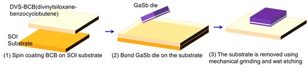
Figure 1: GaSb heterogeneous integration process flow. VCSELs are good candidates for sources in the short-wave infrared, since they can provide valuable characteristics such as low power consumption, small beam divergence, wide tunability and cost-effective packaging. Traditional VCSEL consists of two distributed Bragg reflector (DBR) mirrors parallel to the wafer surface with an active region for the laser light generation in between. Since single-layer high contrast grating (HCG) structure can offer very high reflectivity for a certain spectral band by design, it can be used as to replace the traditional very thick DBR. Freestanding HCGs can be actuated resulting in a change of the resonance wavelength of the cavity. So a widely-tunable electrically-pumped GaSb VCSEL can be fabricated based on a CMOS-compatible HCG mirror and adhesive wafer bonding technology. 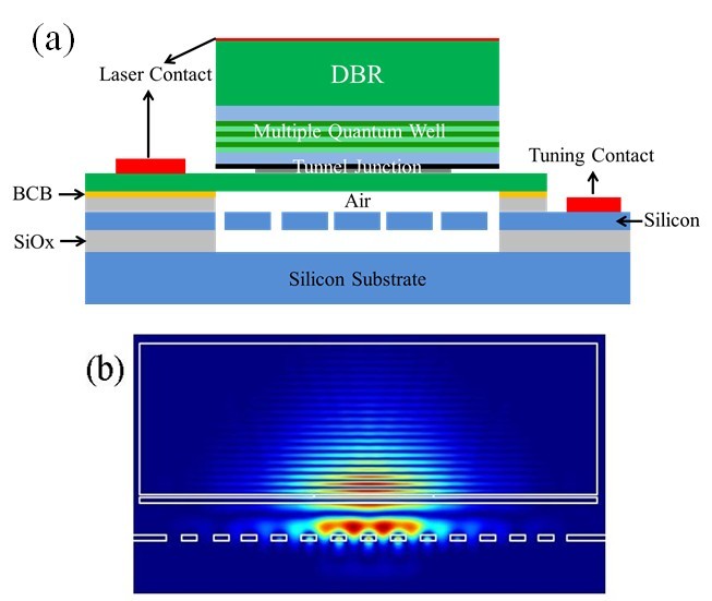
Figure 2: (a) schematic of the widely tunable GaSb/silicon hybrid VCSEL structure based on a high contrast grating as a bottom mirror; (b) Field profile of the resonant mode of the structure. In the telecommunication wavelength range, several III-V on silicon integrated edge-emitting laser structures were developed for silicon photonic circuit light sources. Such structures can however also be realized in the short-wave infrared wavelength rang. Figure 3 shows a GaSb Fabry-Perot laser integrated on a silicon waveguide platform and an SEM cross-section of the fabricated device. 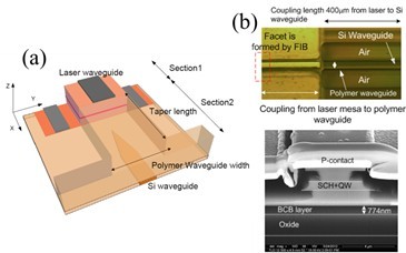
Figure 3: (a) Schematic drawing of the integrated GaSb Fabry-Perot laser, (b) SEM cross-section of the fabricated device. Other people involved: Publications |