|
| |
Focused-ion-beam fabricationMain Researcher: Jonathan Schrauwen
Focused-ion-beam (FIB) is a technology that has been used for quite some years in microelectronics, for device analysis and modification, of for mask repair. The technique is based on ion sputtering with a finely focalized beam of high energy ions (10-100 keV). By adding a gas to the chamber one can also use this beam for deposition of certain materials or for selective etching. In recent years the diameter of the ion beam was decreased towards the nanometer range (currently about 10nm) and commercial systems aiming at nano-modification became available. We are currently hosting an FEI Nova 600 dualbeam FIB in our Clean Room facilities. More information on this system can be found here.
Just like ebeam lithography, FIB is a serial technique, so it will probably not be used for mass fabrication of large area structures. But both techniques have higher resolution than optical lithography and can be used for prototyping or for small modifications to large structures made with conventional techniques. As opposed to ebeam lithography, FIB is a direct write technique. It doesn't need processing steps like resist spinning, resist development or plasma etching. In addition to this FIB allows slanted facet etching and etch depth variations, which greatly enhance design liberty for photonic compontents.

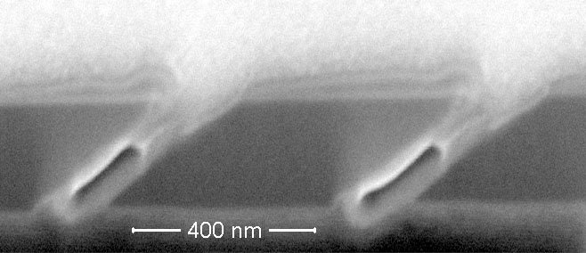
Two slits of a slanted fibre coupler, with sub 100 nm dimensions
However, FIB has the inconvenient problem of damaging the crystal structure of semiconductors. This generates optical losses, which, dependent on the geometry, can be so high that all the light in a structure is absorbed. We have shown that this large excess losses in silicon can be harnessed by using iodine as etch enhancement gas and sapphire as protective mask. This technique has successfully been used to fabricate slanted fiber couplers in silicon-on-insulator waveguides with 46% efficiency (published here).
We are currently experimenting with loss reduction by damage annealing, and we are investigating loss reduction mechanisms in III-V materials. Other people involved: PhD thesises Patents PublicationsInternational Journals
-
S. Vandewiele, T. Brans, L. Van Landschoot, K. Komorowska, S. Verstuyft, A. Subramanian, C. Hu, F. Beunis, R. Baets,
Single mode air-clad liquid-core waveguides on a surface energy patterned substrate, Optics Letters, 39(16), p.4942-4945 doi:10.1364/ol.39.004942 (2014)
 . . -
J. Schrauwen, J. Van Lysebettens, T. Claes, K. De Vos, P. Bienstman, D. Van Thourhout, R. Baets,
Focused-ion-beam fabrication of slots in silicon waveguides and ring resonators, IEEE Photonics Technology Letters, 20(23), p.2004 doi:10.1109/lpt.2008.2006001 (2008)
 . . -
J. Schrauwen, D. Van Thourhout, R. Baets,
Iodine enhanced focused-ion-beam etching of silicon for photonic applications, Journal of applied physics, 102, p.103104 doi:10.1063/1.2815664 (2007)
 . . -
J. Schrauwen, F. Van Laere, D. Van Thourhout, R. Baets,
Focused-ion-beam fabrication of slanted grating couplers in silicon-on-insulator waveguides, Photonics Technology Letters, 19(11), p.816-818 doi:10.1109/lpt.2007.897293 (2007)
 . . -
J. Schrauwen, D. Van Thourhout, R. Baets,
Focused-ion-beam fabricated vertical fiber couplers on silicon-on-insulator, Applied Physics Letters, 89, p.141102 doi:10.1063/1.2356311 (2006)
 . .
International Conferences
-
J. Schrauwen, S. Scheerlinck, D. Van Thourhout, R. Baets,
Polymer wedge for perfectly vertical light coupling to silicon , SPIE Photonics West, 7218, United States, p.72180B (8 pages) doi:10.1117/12.807558 (2009)
 . . -
J. Schrauwen, J. Van Lysebettens, M. Vanhoutte, D. Van Thourhout, R. Baets,
Iodine enhanced FIB etching of silicon for photonic device modification and prototyping, Fib for photonics (invited), Netherlands, p.4-7 (2008)
 . . -
J. Schrauwen, D. Van Thourhout, R. Baets,
Trimming of silicon ring resonator by electron beam induced compaction, ECIO 2008, (2008)
 . . -
J. Schrauwen, G. Roelkens, D. Van Thourhout, R. Baets,
Focused-ion-beam lithography for prototyping of silicon photonic compontnets, EIPBN, United States, (2008)
 . . -
J. Schrauwen, E.J. Klein, F. Ay, W.C.L. Hopman, R.M. De Ridder, D. Van Thourhout, R. Baets,
Reducing optical losses in focused-ion-beam etched silicon by annealing, EIPBN, United States, (2008)
 . . -
J. Schrauwen, E. Klein, R. De Ridder, W. Hopman, D. Van Thourhout, R. Baets,
Reducing optical losses in focused-ion-beam etched silicon by annealing, ePIXnet annual meeting 2007 (invited), Spain, (2007)
 . . -
S. Scheerlinck, J. Schrauwen, D. Taillaert, D. Van Thourhout, R. Baets,
Efficient, broadband and compact metal grating couplers fo silicon-on-insulator, CLEO/QELS 2007, United States, (2007)
 . . -
J. Schrauwen, F. Van Laere, D. Van Thourhout, R. Baets,
Focused-ion-beam fabrication of slanted fiber couplers in silicon-on-insulator waveguides, ECIO 2007, Denmark, (2007)
 . . -
J. Schrauwen, D. Van Thourhout, R. Baets,
Focused ion beam for photonics, a new versatile fabrication method, ePIXnet winterschool 2007, Switzerland, (2007)
 . . -
J. Schrauwen, F. Van Laere, D. Van Thourhout, R. Baets,
Focused-ion-beam fabrication of slanted fiber couplers in silicon-on-insulator waveguides, Leos Benelux, (2006)
 . . -
J. Schrauwen, D. Van Thourhout, R. Baets,
Focused-Ion-Beam Fabricated Vertical Fiber Couplers on Silicon-on-Insulator Waveguides, IEEE Group IV Photonics, P20, Canada, doi:10.1109/group4.2006.1708179 (2006)
 . . -
J. Schrauwen, D. Van Thourhout, R. Baets,
Reducing optical losses in devices fabricated with focused ion beam, ePIXnet wintershool 2006 , Switzerland, (2006)
 . .
National Conferences
-
J. Schrauwen, D. Van Thourhout, R. Baets,
Focused ion beam for photonics: a new versatile fabrication method, 7e UGent-FirW Doctoraatssymposium, interactive poster session, Belgium, p.paper nr. 20 (2006)
 . .
Back to overview
|
